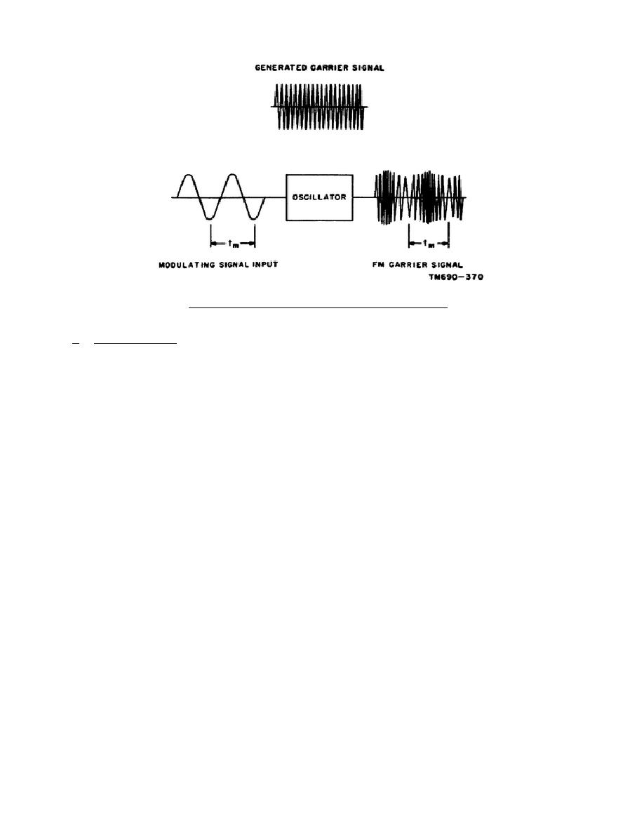
Figure 2-1.
FM oscillator, block diagram.
b. FM Oscillator.
(1) A typical FM oscillator stage is shown in figure 2-2.
In this
application, the modulation is established by reactance modulation.
The
modulating signal, coupled through transformer T2, varies the emitter-base
bias of reactance modulator Q2.
Since the bias is increasing and
decreasing at the modulation rate, the collector voltage also increases
and decreases at the modulating rate. As the collector voltage increases,
output capacitance CCE decreases, and as the collector voltage decreases,
output capacitance CCE increases. When output capacitance CCE increases,
the resonant frequency of the oscillator Q1 tank circuit (capacitor C1 and
winding 1-3 of transformer T1) increases.
When output capacitance CCE
increases, the resonant frequency of the oscillator tank circuit
decreases.
The resonant frequency of the oscillator tank circuit is
therefore increasing and decreasing at the modulating rate, as does the
frequency of the signal generated by the oscillator.
The output of the
oscillator is an FM carrier signal.
(2) Transistor Q1 provides the oscillator signal. Capacitor C1 and winding 1-
3 of transformer T1 form a parallel resonant circuit for the oscillator
frequency. Winding 4-5 of transformer T1 provides the required feedback,
and winding 6-7 couples the oscillator signal to the following stage.
Transformer T2 couples the modulating signal to reactance modulator Q2.
The reactance of output capacitance CCE across winding 2-3 of transformer
T1 varies the resonant frequency of the oscillator tank circuit (capacitor
C1 and winding 1-3 of transformer T1).
10


 Previous Page
