to the emitter through ground and R3 (the stabilizing resistor).
This current
causes a voltage drop of 2.1 volts across R3, which reduces the forward bias
between base and emitter to the difference between +2.5 and +2.1 volts (base minus
emitter voltages), or +0.4 volt.
This small voltage is increased by the AGC
voltage connected to the emitter when a strong signal is received. Thus, a strong
signal causes the AGC voltage to become more positive; this increases the emitter
positive voltage, thereby reducing stage gain.
c. Output Signal Path.
The +6.5 volts applied to the collector circuit is
reduced to +5 volts at the collector because of the voltage drop in the collector
series resistors R4 and R5. The collector-current signal variations appear across
L2 and the collector resistors.
Note that capacitors C1 and C3 are ganged to
achieve tracking. Tank circuit L2-C5, tuned by C3, forms a high-impedance output
circuit. Resistor R4 and capacitor C6 combine to form a low-impedance circuit to
match the impedance of the mixer circuit.
2-3.
MIXER
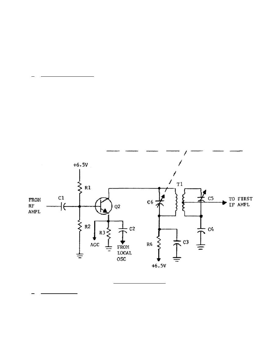
A mixer stage using an NPN transistor is shown in figure 2-2.
Like the RF
amplifier just described, this mixer uses a grounded emitter common to both input
and output (base and collector) circuits.
Figure 2-2.
Mixer.
a. Input Circuit. The input circuit receives the signal from the RF amplifier
through coupling capacitor C1. The signal voltage developed across R2 is impressed
across the base-emitter junction. The local oscillator signal that is to be mixed
with the input RF signal is coupled into the emitter-base junction by capacitor C2.
322 L2
8


 Previous Page
