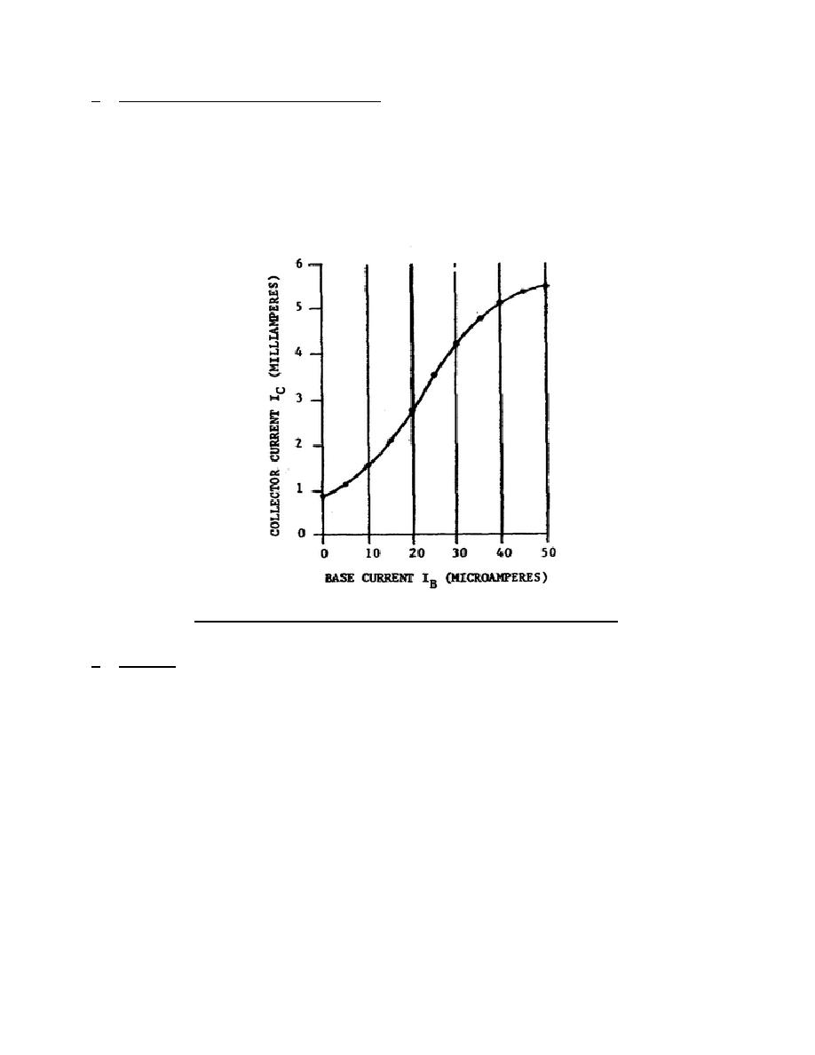
b. Transistor Characteristic Curve.
Transistors have characteristic curves
similar to the curves for electron tubes. In figure 2-3 the characteristic curve
(base current vs collector current) shows that at the high and low current portions
of the curve (IB = 0 to 10 and 35 to 50 microamperes) the amount of collector
current change is not the same for each microampere of change in base current. The
curve is nonlinear in these areas.
Between the extremes (IB = 10 to 35
microamperes), the collector current will change approximately the same amount for
each microampere of change in base current.
This portion of the characteristic
curve is linear.
Figure 2-3.
Typical transistor characteristic curve.
c. Biasing. In figure 2-2, a voltage-dividing network consisting of R1 and R2
in series with the +6.5-volt supply biases the emitter-base junction to +1.6 volts.
The collector current flowing through stabilizing resistor R3 produces +0.85 volt,
which opposes the +1.6 volts and makes the total bias voltage +0.75 volt.
The
transistor is being biased in the low-current region, producing nonlinear
characteristics.
As the local oscillator voltage swings from one signal peak to
another, the emitter voltage will change.
The negative swing of the oscillator
voltage will oppose the 0.85-volt drop across R3, thus providing less opposition to
the +1.6 volts at the base-emitter junction. This increases the forward bias and
causes the transistor to conduct more heavily (not to saturation).
The positive
swing of the oscillator voltage aids the +0.85-volt drop across R3, providing more
opposition to the +1.6 volts at the junction. This decreases the forward bias and
causes the transistor to conduct less heavily (not to cutoff). As the transistor
passes
322 L2
9


 Previous Page
