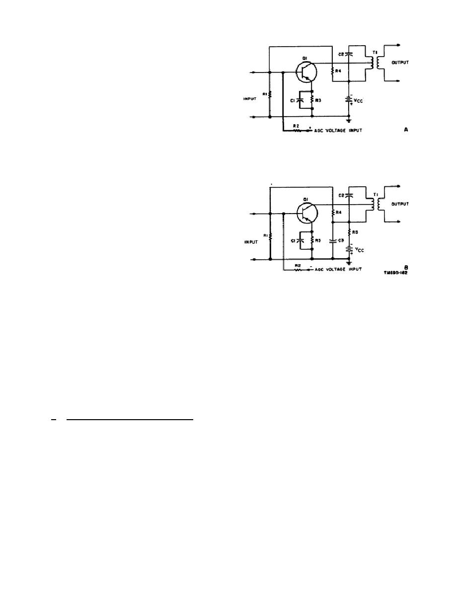
(1) In
this
case,
the
tuned
amplifier is also operating
as a dc amplifier to increase
the dc current output of the
second detector.
If the dc
current output of the second
detector
is
sufficiently
large, the dc emitter current
of the tuned amplifier may be
varied directly.
(2) In the circuit, resistors R1
and R4 form a voltage divider
and establish the no signal
negative (forward) bias on
the base.
The AGC voltage
input
from
the
second
detector
is
positive
with
respect to ground and is fed
to the base through dropping
resistor R2.
When the dc
output of the second detector
increases (because of a high
carrier signal input to the
detector), the positive dc
voltage fed to the base of
Q1
through
dropping resistor R2 reduces
the net negative (forward)
bias
on
the
base
and
Figure 4-1. Common-emitter amplifier
decreases
the
emitter
with AGC.
current.
The gain of the
amplifier is also decreased.
When the dc output of the second detector decreases, the net forward bias
of Q1 increases and increases the emitter current.
The gain of the
amplifier increases.
(3) Resistor R3, ac bypassed by capacitor C1, is the emitter-swamping
resistor. Capacitor C2 and the primary of transformer T1 form a parallel
tuned circuit to develop the collector input signal.
Transformer T1
matches the collector output of Q1 to the input of the following stage.
The primary of T1 is tapped to obtain the desired amplifier selectivity
(Qo).
b. Dc Collector Voltage Control. The power gain of the common-emitter amplifier
shown in B of figure 4-1 is controlled by feeding the AGC voltage to the base of
the amplifier to vary the dc emitter current which, in turn, varies the dc
collector voltage.
The dc collector voltage is varied by passing the collector
current through resistor R5. To be effective, resistor R5 must be 10,000 ohms or
higher in value.
(1) In this case, the tuned amplifier is also operating as a dc amplifier to
increase the dc output voltage of the second detector. If the dc voltage
output of the second detector is sufficiently large, the dc collector
voltage of the tuned amplifier may be varied directly.
39


 Previous Page
