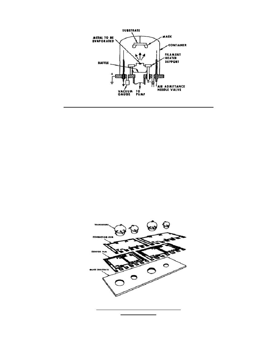
Figure 3-8.
Vacuum evaporation forming a thin film IC.
(1) A process known as vacuum evaporation is often used to form a thin film
IC. This method is shown in figure 3-8. Here you see a small piece of
metal inside a container.
Directly above the metal is the substrate
with a mask attached.
The mask, similar to the ones used with
monolithic IC's, determines the pattern of the deposited film. A high
vacuum is created in the container and the metal is heated to its
boiling point.
As the metal boils, its vapor condenses on the
substrate through the openings in the mask.
This process is repeated
with different materials and masks until all the required resistors,
capacitors, and conductors are formed.
Unlike the monolithic IC, in
which transistors are formed as part of the epitaxial layer, the thin
film IC has miniature diodes or transistors attached to the circuit.
Figure 3-9 is an exploded view of a thin film IC.
If capacitors are
needed in this circuit, they are deposited as a separate film.
(2) In the thin film process it is possible to make resistors and
capacitors with higher values and closer tolerances than those in
monolithic IC's.
For this reason, thin film IC's are preferred for
high-frequency circuits that require precision components.
Figure 3-9. Exploded view of a
thin film IC.
309 L3
46


 Previous Page
