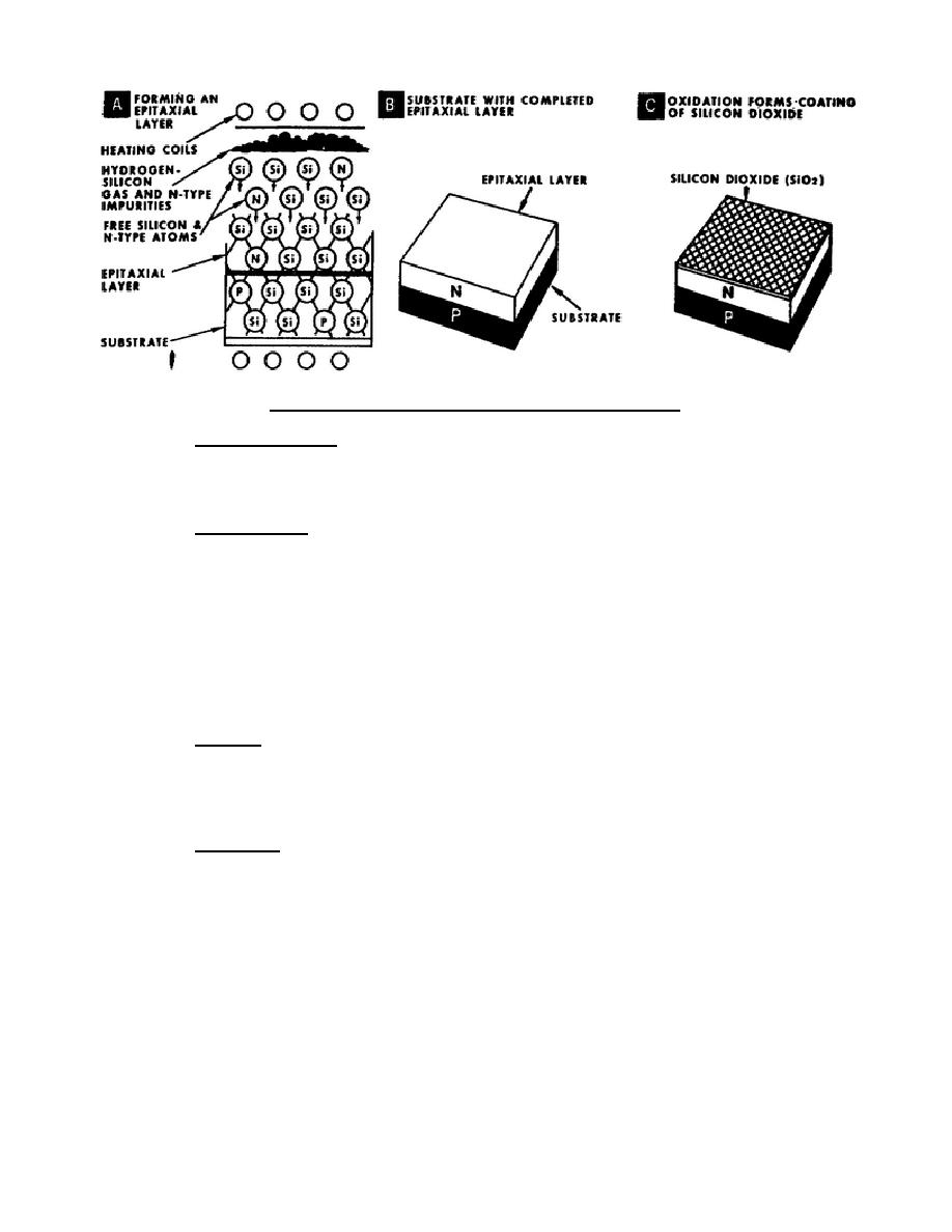
Figure 3-4.
Epitaxial growth and oxidation.
(2) Completed layer. After the epitaxial growth is completed, the chip is
heated and exposed to wet oxygen gas, which causes a protective silicon
dioxide (SiO2) coating to form on the chip. The crystal with a layer of
SiO2 is shown in C of figure 3-4.
(3) Photomasking. The chip is now coated with a solution of photoresist as
shown in A of figure 3-5. Photoresist leaves a coating that will not
dissolve in photo developing fluid after it has been exposed to
ultraviolet light. A glass slide called a photomask is aligned on the
chip as shown in B of figure 3-5.
The photomask contains light and
dark areas similar to a photo negative.
The chip is exposed to
ultraviolet light and then washed with photo developing fluid to
dissolve the photoresist under the dark areas of the photomask.
The
results of the photofluid bath are shown in C.
Notice that the only
areas of photoresist that remain are those not protected by the
photomask.
(4) Etching.
The uncovered SiO2 is removed by etching.
An acid bath
removes the bare SiO2 without affecting the epitaxial layer or the SiO2
in the two areas where the photoresist remains. This step is shown in
D of figure 3-5.
After the etching, the remaining photoresist is
stripped from the chip as shown in E.
(5) Diffusion.
The chip is placed in a furnace with a precise number of
impurity atoms (dopant). At about 1,200 C, the impurity atoms diffuse
into the epitaxial layer.
Figure 3-6 shows the chip in the various
stages of diffusion.
The diffusion is rigidly controlled so that it
can be stopped when impurity atoms reach the substrate. Notice in C of
figure 3-6 that the diffusion does not affect the silicon directly
below the protective SiO2, which isolates these areas from diffusion.
This process is known as isolation diffusion.
309 L3
42


 Previous Page
