2.
THEORY OF OPERATION.
This portion of the lesson is devoted to examination of each of the
major circuits comprising the Model 5345A counter.
Signal processing for
each of the various functions is explained in the paragraphs describing Main
Gate operation.
Throughout the circuit descriptions, refer to the block
diagram of figure 2 as well as each of the individual figures as they appear
in the text.
a. Input Assembly. The counter has two input channels (A and B), each
having a frequency range of dc to 500 MHz.
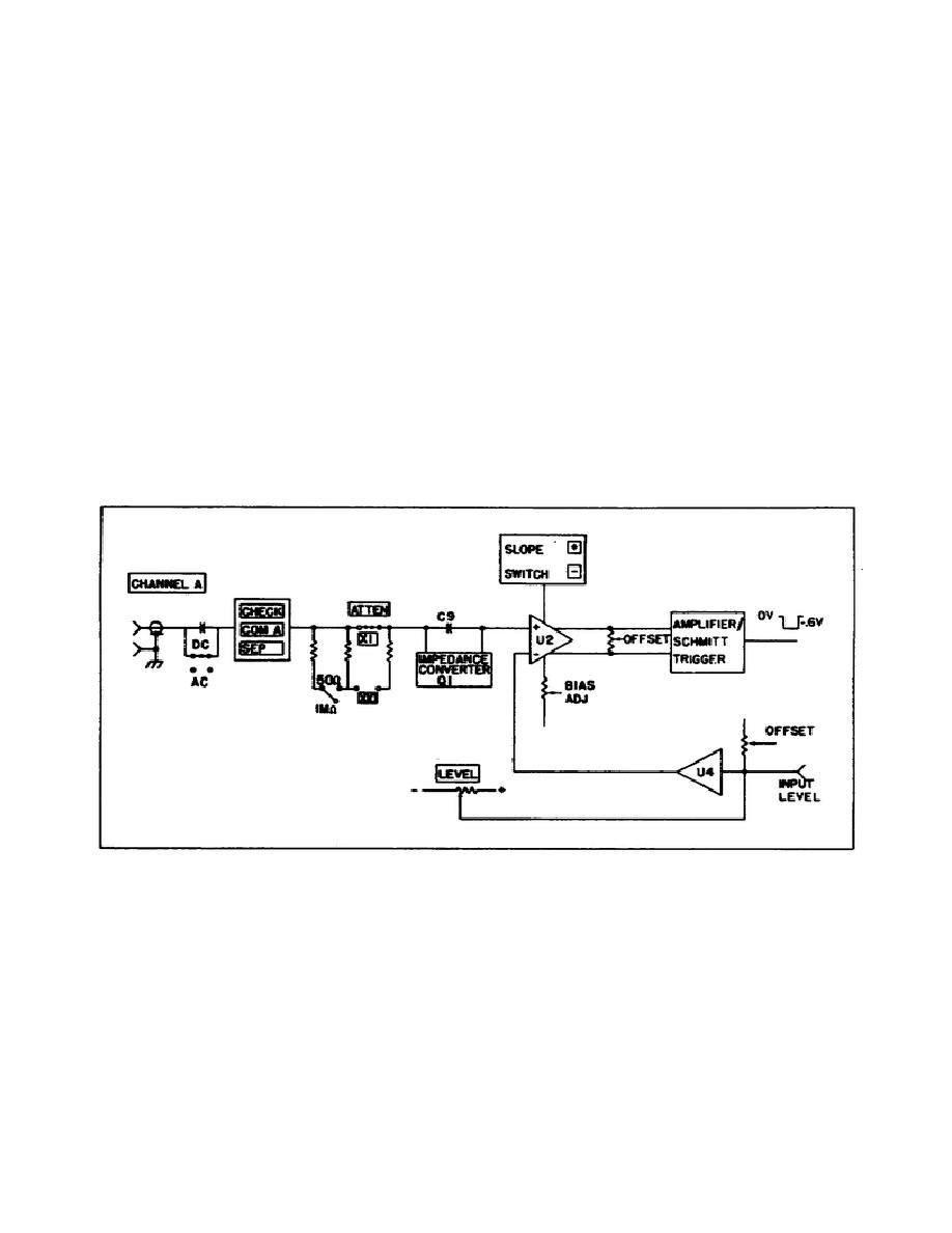
Figure 3 is a simplified
representation of Channel A input circuitry. AC coupling is accomplished by
switching a capacitor in series with the input signal. When DC coupling is
selected, the capacitor is shorted out.
With the Input Amplifier Control
set to CHECK, a 100 MHz test signal is connected into the circuit. When in
COM A, channels A and B are connected in parallel. When in SEP, the input
signal is connect directly to the attenuator. When 50 ohm input impedance
is selected, a selected value of resistance (49.9 ohms) parallels the input
attenuators. The attenuator switch passes the signal directly in X1 or when
in X10 attenuates the signal by 10 through a divider network.
Figure 3.
Simplified input circuit.
The signal is then routed to the first amplification stage through one
of two paths, depending on the frequency.
Frequencies below 10 MHz,
including do, pass through the FET impedance converter (source follower).
Higher frequencies are bypassed around the FET through C9. The amplifier U2
has differential inputs and outputs and has a gain (single-ended) of about
3. One input accepts the signal and the other accepts the dc level
39


 Previous Page
