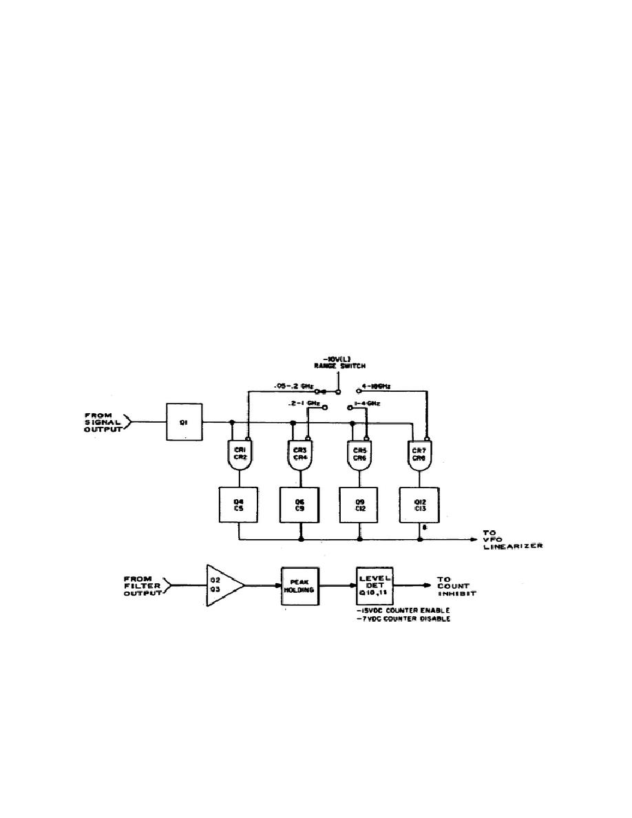
(7) Automatic Phase Control No. 2.
Referring back to the block
diagram, the signal output from the variable gain amplifier of APC No. 1 is
routed to the range compensation circuit of APC No. 2.
Also, the signal
from the 1 kHz filter is fed to the amplifier and level detector. Figure 10
is a simplified representation of the two circuits comprising APC No. 2.
The major purpose of this circuit is to detect the 1 kHz signal in the APC
loop and to change the gain of the APC loop to compensate for oscillator
nonlinearity in the different ranges.
The filtered 1 kHz from the sampler is amplified by Q2 and Q3 and sent
to a peak holding circuit which works just like the one discussed in para 6.
The peak detected signal is then sent to a level detector made up of Q10 and
Q11.
When the output of Q11 is -15V (Q11 off), the signal from the
prescaler (block diagram) is sent to the counter.
This condition is
desirable when phase locked in the APC mode or when in the Pulsed RF mode.
When Q11 is on, its collector goes to -7V and the prescaler disabled.
The range compensation circuit consists of Q1 and four similar
configurations, one for each available range.
When range .05 to .2 is
selected, -10V back biases CR1 and forward biases CR2. Q4 and C5 become the
collector load for Q1 and the signal is fed to the VFO linearizer. The gain
is changed for each of the different ranges.
Figure 10.
Automatic phase control no. 2.
73


 Previous Page
