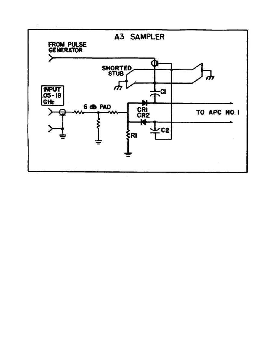
Figure 5.
Sampler assembly.
(4) Automatic Phase Control (APC) No. 1. At the gate of Q2A (figure
6) is the algebraic sum of the voltages on C1 and C2 of the sampler. Q2A is
a source follower that provides minimum loading due to the extremely high
impedance of the FET.
Q3 provides an in-phase signal to Q2A's drain to
effectively reduce drain to gate capacitance. Q2B provides a dc reference
voltage to the base of QS5. When in the APC mode, a 1 kHz signal from the
collector of Q4 is also sent to the gate of Q2B. The sampler signal from
the source of Q2A is amplified by Q7, and the do and 1 kHz reference signal
are amplified by Q5. Q6A and Q6B are current sources for Q5 and Q7. The
front panel Level Adj varies the emitter resistance of Q5 and Q7. When the
resistance of R1 decreases the gain increases and vice-versa.
Q8 and Q9
form a balanced dc amplifier.
The output of Q8 goes to the front panel
output jack and will be the amplitude of the zero beat. The output of Q11A
goes to the front panel meter mode switch. The output of Q9 is the error
voltage if in APC mode or the beat amplitude if in pulsed RF. This output
goes to the APC control No. 2 and to the peak holding circuit for PRF. Q12
and associated circuits detect the kHz reference signal. This output goes
td another peak holding circuit which holds the peak amplitude of the 1 kHz
signal to drive the inhibit amplifier.
69


 Previous Page
