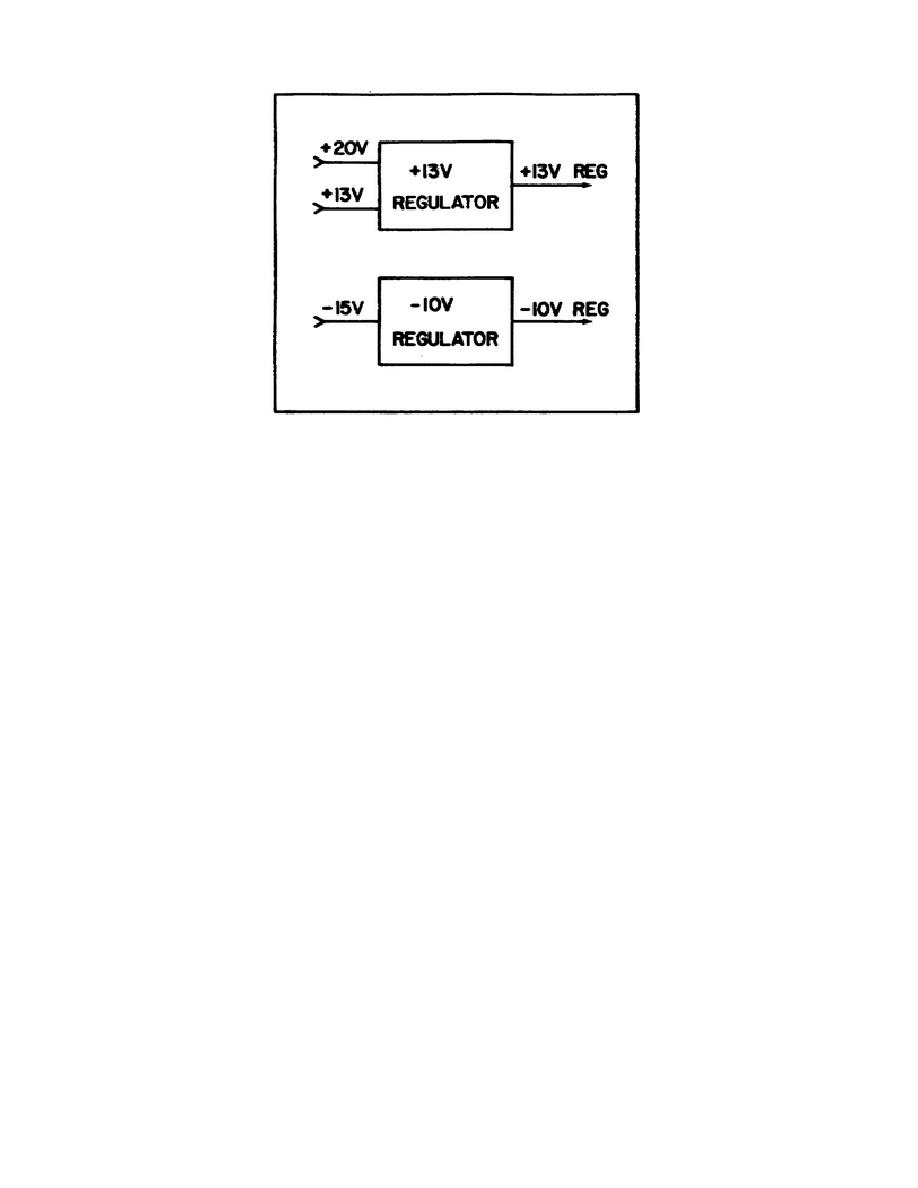
Figure 7.
Simplified regulator circuit.
Transistor Q10 (figure 8) amplifies the reference signal from the
emitter of Q8 in APC No. 1 and provides the pulsed RF output to the front
panel of the transfer oscillator.
The connection in a Common Collector
configuration results in a high input impedance and provides good signal
isolation.
(6) Peak Holding and DC Amplifier. The peak holding circuit (figure
9) detects the peak-to-peak signal from the base of Q11B on APC No. 1 and
passes it to the front panel meter. The APC signal is amplified by Q1 and
Q2 and ac coupled by C1 to the base of Q3A. Q3A and Q3B are connected as a
The signal on the collector of Q3A is coupled to
the base of Q7 which drives emitter follower Q6. The output of Q6 charges
C2 and, because of the long time constant of C2 and R9, C2 holds the level
of the pulses.
Q4 and Q5 form a Darlington amplifier and provide a high
input impedance to minimize any loading effect on C2.
The resultant dc
level on the bases of Q3B and Q8A is the voltage charged on C2 plus the
junction voltage drops of Q4 and Q5. Since Q3A and Q3B are emitter coupled,
this dc voltage is compared with the input on the base of Q3A.
This
difference drives Q7 and the process continues until the loop has stabilized
at peak voltage.
The voltage on the base of Q8A receives amplification by Q8B.
Q8A
conducts heavily with no input while Q8B is virtually held off; no current
flows through R15 and the meter does not deflect.
With a negative going
input signal, however, Q8A starts turning off and emitter
71


 Previous Page
